STM32F103 Development Board
Schematic
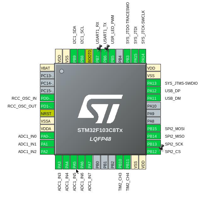
The following schematic is for a STM32F103C8 32 bit microcontroller by STMicroelectronics. I was drawn to the STM32 family due to my familiarity with it from university. The board is simple, featuring a 16MHz crystal and a USB type C connector connected using the USB2.0 spec. The pins of the microcontroller are highly configurable. I planned for the board to support as many simultaneous functions as possible, hence I designed the board with the following pin layout in mind. Of course, this can be largely ignored and another pin layout can be planned with the STM32CubeIDE utility.
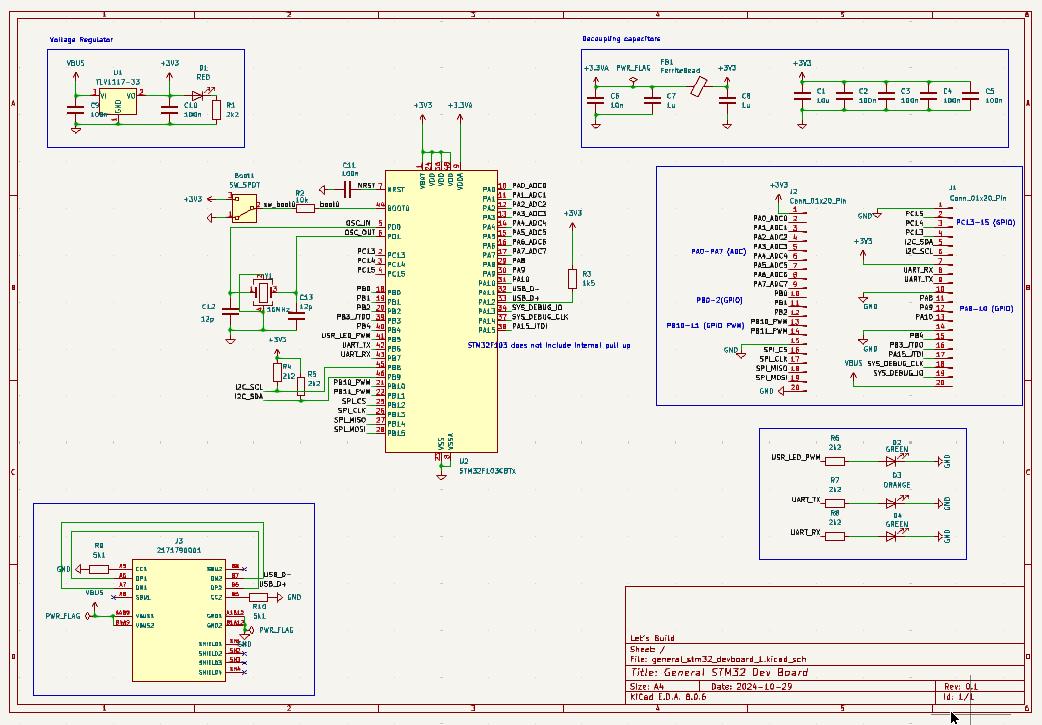
The final board schematic is as follows:
PCB Design
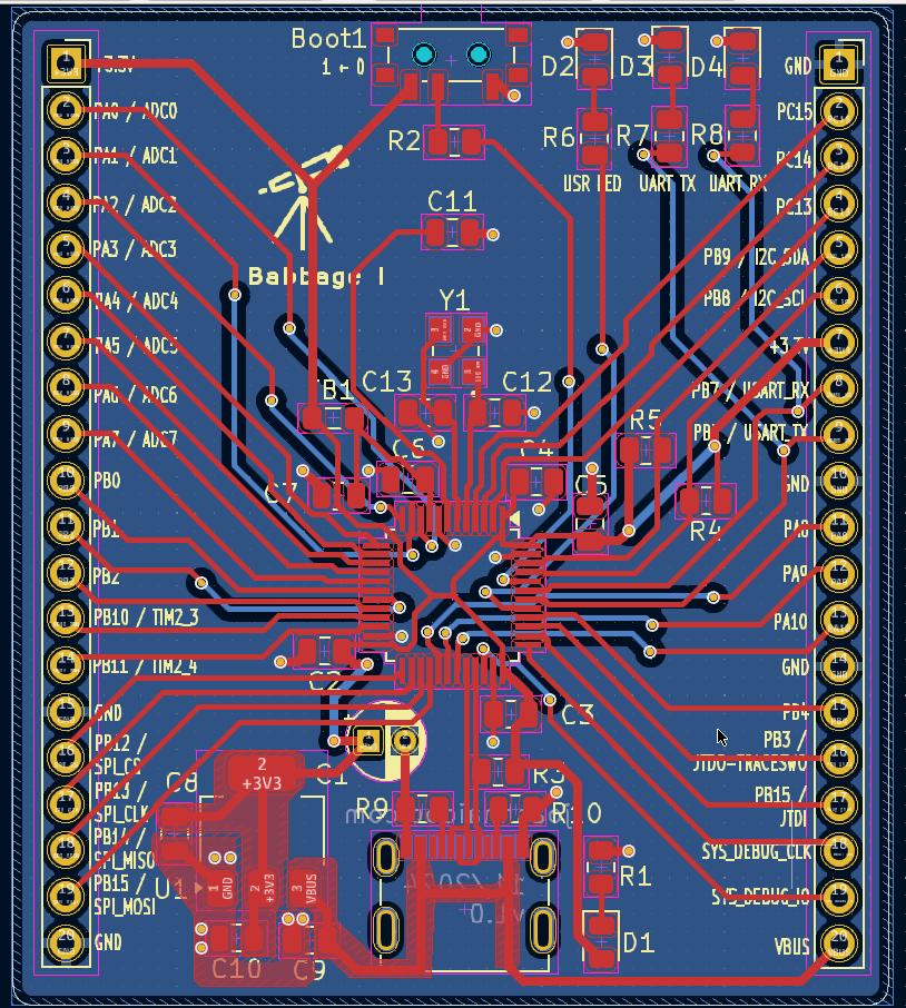
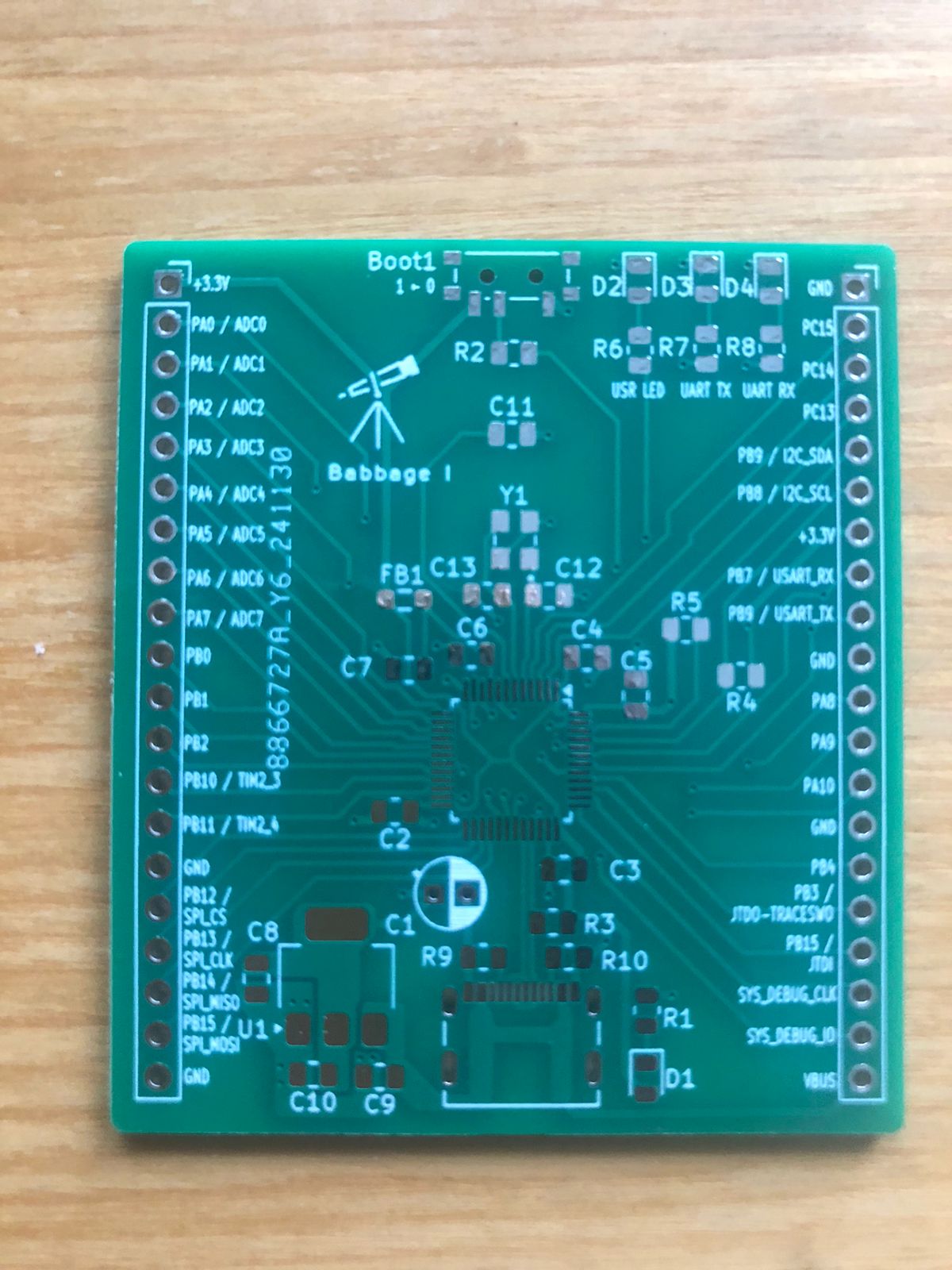
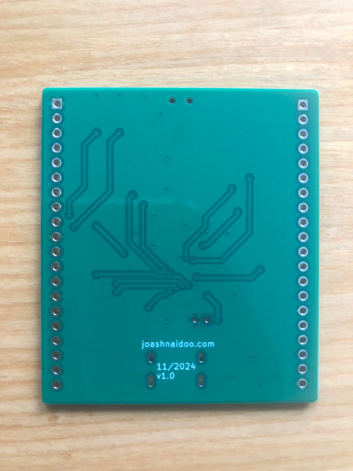
Matching the simplicity of the schematic, the PCB contains only two layers. The first for routing signal traces, and the bottom acting as a ground plane. The signal traces measures 0.3mm and 0.5mm for the power traces. Vias to the ground plane had a diameter of 0.7mm and hole diameter of 0.4mm. The outer dimensions of the board measured 48mm x 54.5mm.
PCB Manufacturing
The board was manufactured at JLCPCB using FR-4 material with a thickness of 1.6mm.
PCB Assembly
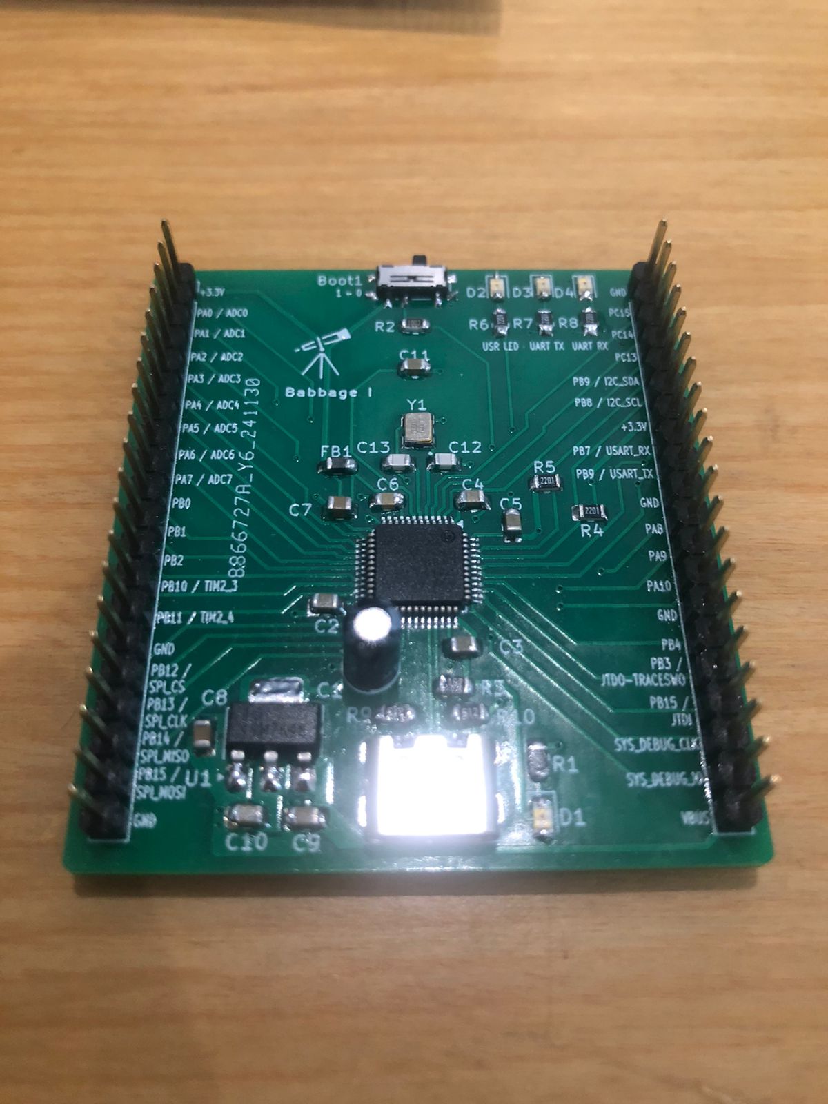
Most of the components were chosen to be 0805 size and hence easy for hand soldering.
Board bring up
The boot switch allows us to program the STM32 microcontroller’s built in flash memory. When the switch is pulled high, we can write an .elf file to flash memory over UART using ST Electronics’ STM32CubeProgrammer utility. Since the external oscillator is 16MHz, the baud rate is 115200 with even bit parity. I used my previously designed USB to UART PCB to bridge between my PCB and the STM32.

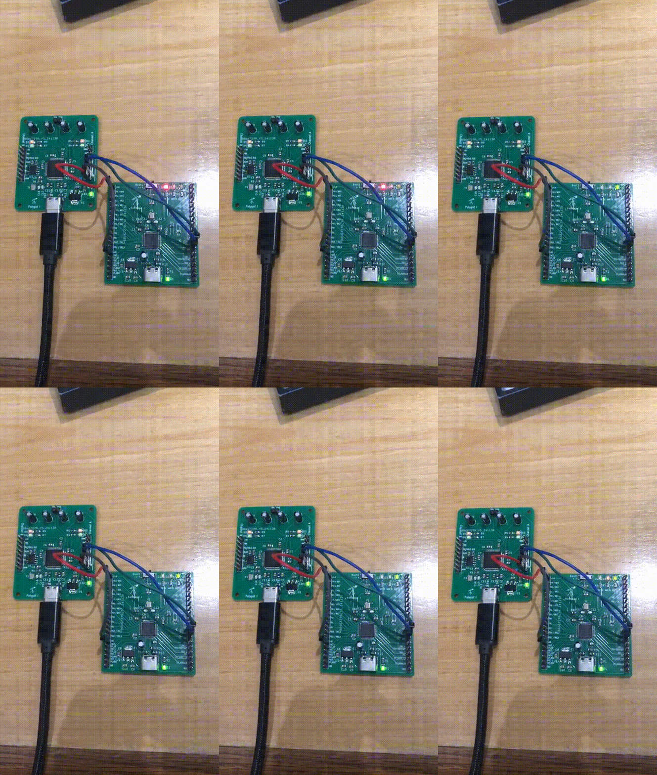
As a demo application, I flashed a simple program to iterate through the 3 user LEDs in quick succession. The .GIF below shows this in action.
