FT2232H Breakout Board
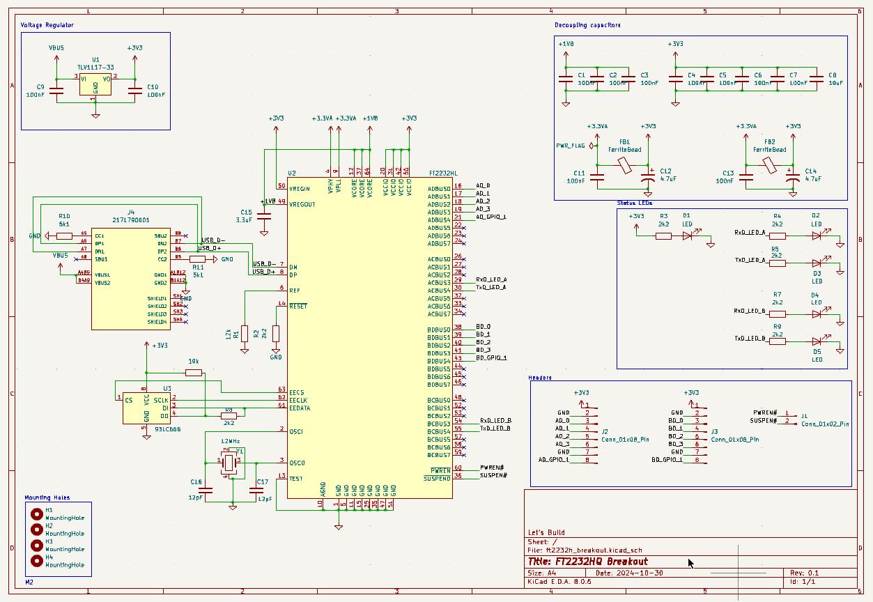
Schematic
This project is a breakout board for FTDI’s FT2232H IC which provides a independent dual channel USB to UART / SPI / I2C / JTAG conversion. The entire project was developed with KiCAD, an open source PCB design software. Other notable PCB design features include:
- a USB type C connector, connected using the USB 2.0 spec
- 12MHz crystal oscillator
- 93LC66B Microchip 4KB EEPROM for programming (required for independent channel control)
PCB Design
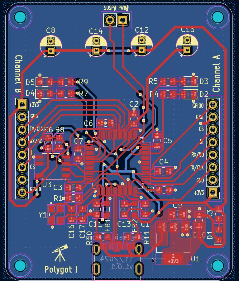
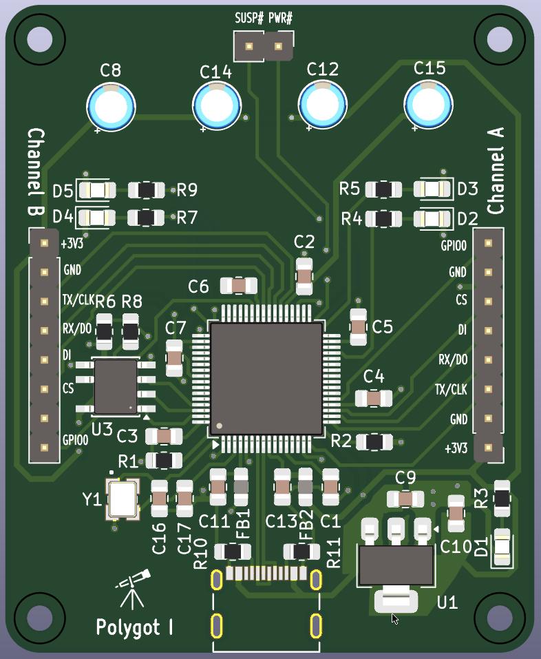
The PCB is a two layer board with the top layer for signal and power routes and the bottom layer as a ground plane. The signal traces measures 0.3mm and 0.5mm for the power traces. Vias to the ground plane had a diameter of 0.7mm and hole diameter of 0.4mm. Signal and via dimensions were chosen specifically to meet manufacturer’s capabilities. Most passive SMD components were given an 0805 size for easy hand soldering later. The PCB layout and render are given below.
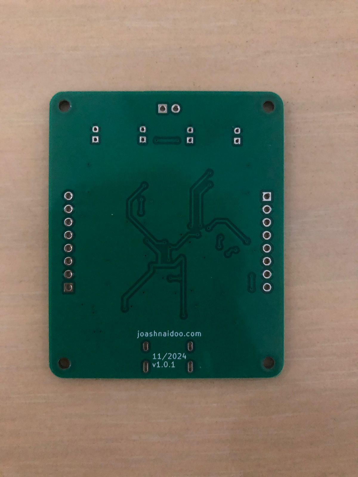
PCB Manufactured
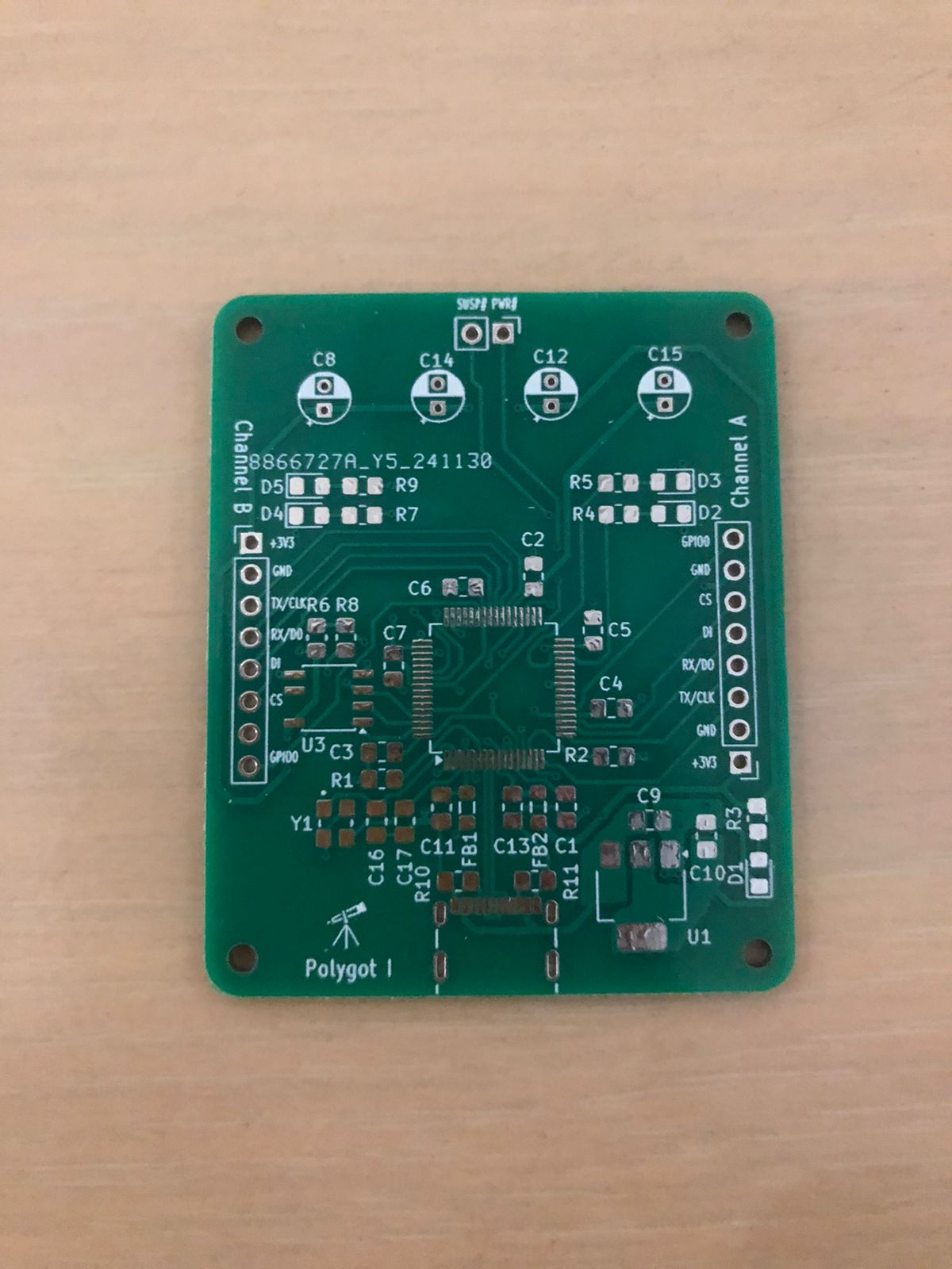
The PCB was manufactured with JLCPCB in China using FR-4 material (most common). The outer dimensions of the board measured 46 mm x 56.3 mm.
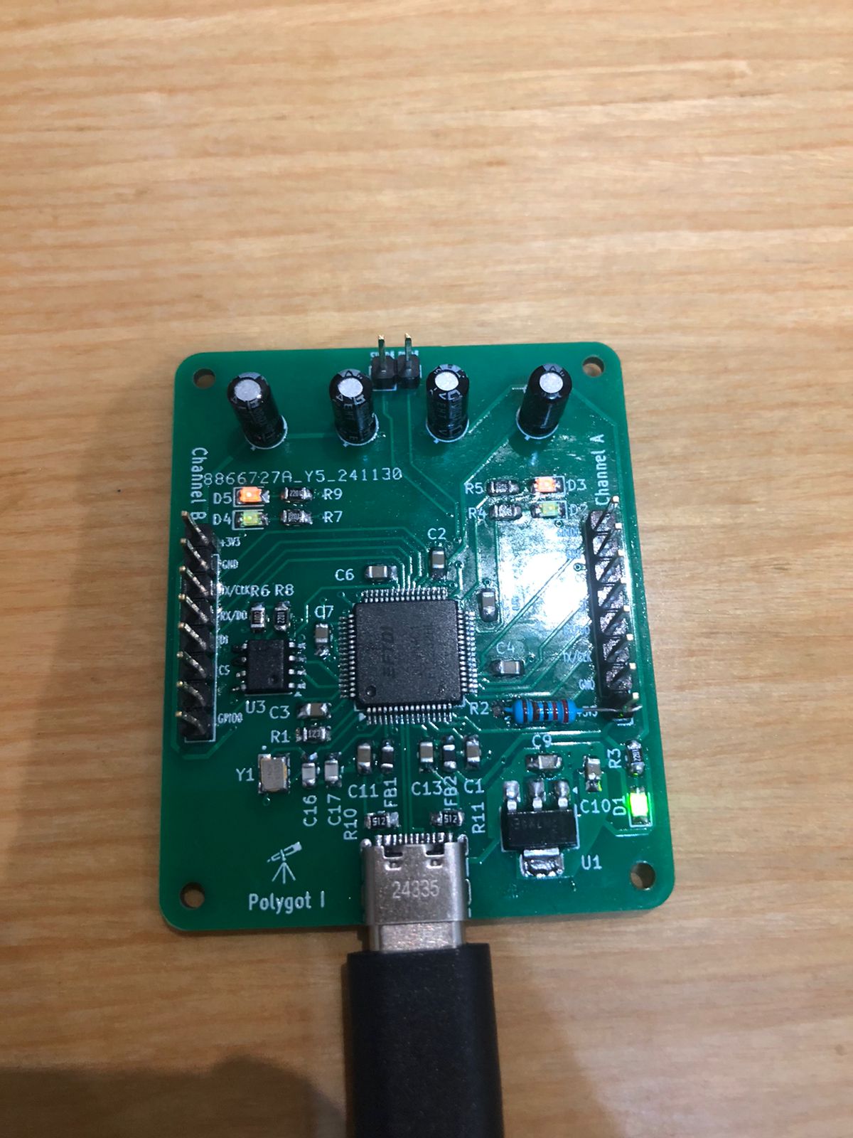
Populated PCB
Components, thanks to being mainly 0805 size, could be hand soldered onto the board. You may notice, for R2, a through-hole resistor instead of the SMD one. This is due to noticing an error in my schematic design, where I tied the active low reset pin to ground instead of VCC leaving the board in permentant reset state. To overcome this mistake, I soldered one end of a through-hole resistor to the appropriate side of the SMD pad and the other end of the resistor to a nearby 3.3V GPIO pin.
Board bring up
FTDI provides open source drivers built into the Linux kernel itself. They also provide a dotnet application for flashing to the EEPROM memory. Below, we see the board appearing on dmesg and lsusb respectively.

